- 您现在的位置:买卖IC网 > Sheet目录476 > MDEV-900-HP3-PPS-RS232 (Linx Technologies Inc)KIT MASTER 900MHZ HP-3 SIP RS232
�� �
�
�THE� DATA� OUTPUT�
�The� DATA� line� outputs� recovered� digital� data.� It� is� an� open� collector� output� with�
�an� internal� 4.7k� Ω� pull-up.� When� an� RF� transmission� is� not� present,� or� when� the�
�TIMING� CONSIDERATIONS�
�There� are� four� major� timing� considerations� to� be� aware� of� when� designing� with�
�the� HP3� Series� receiver.� These� are� shown� in� the� table� below.�
�received� signal� strength� is� too� low� to� ensure� proper� demodulation,� the� data�
�output� is� squelched� continuous� high.� This� feature� supports� direct� operation� with�
�UARTs,� which� require� their� input� to� be� continuously� high.� An� HP3� transmitter� and�
�receiver� can� be� directly� connected� between� two� UARTs� without� the� need� for�
�buffering� or� logical� inversion.� It� should� be� noted� that� the� squelch� level� is� set� just�
�Parameter�
�T1�
�T2�
�T3�
�T4�
�Description�
�Time� between� DATA� output� transitions�
�Channel� change� time� (time� to� valid� data)�
�Receiver� turn-on� time� via� PDN�
�Receiver� turn-on� time� via� V� CC�
�Max.�
�20.0mS�
�1.5mS�
�3.0mS�
�7.0mS�
�over� the� receiver’s� internal� noise� threshold.� Any� external� RF� activity� above� that�
�threshold� will� “break� squelch”� and� produce� hashing� on� the� line.� While� the� DATA�
�line� will� be� reliably� squelched� in� low-noise� environments,� the� designer� should�
�always� plan� for� the� potential� of� hashing.�
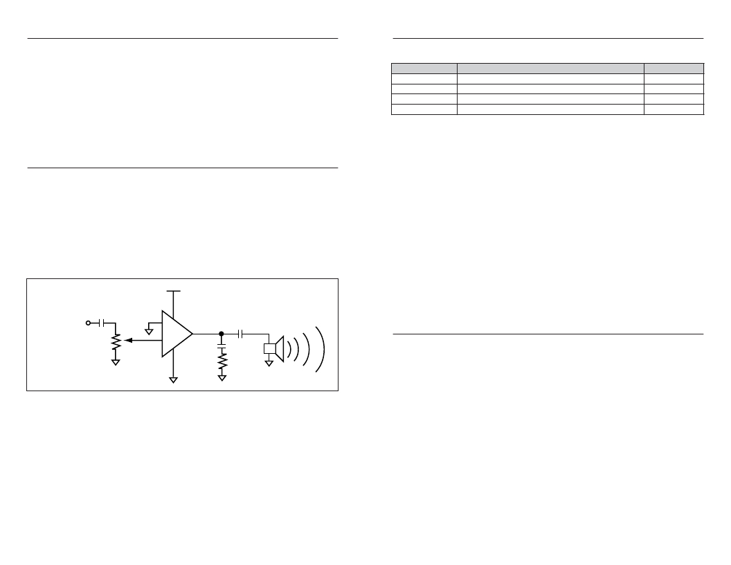
�AUDIO� OUTPUT�
�The� HP3� Series� is� optimized� for� the� transmission� of� serial� data;� however,� it� can�
�also� be� used� very� effectively� to� send� a� variety� of� analog� signals,� including� audio.�
�The� ability� of� the� HP3� to� send� combinations� of� audio� and� data� opens� new� areas�
�of� opportunity� for� creative� design.�
�The� analog� output� of� the� AUDIO� line� is� valid� from� 50� Hz� to� 28� kHz,� providing� an�
�AC� signal� of� about� 1V� peak-to-peak.� This� is� a� high� impedance� output� and� not�
�suitable� for� directly� driving� low-impedance� loads,� such� as� a� speaker.� In�
�applications� where� a� low� impedance� load� is� to� be� driven,� a� buffer� circuit� should�
�always� be� used.� For� example,� in� the� case� of� a� speaker,� a� simple� op-amp� circuit�
�such� as� the� one� shown� below� can� be� used� to� act� as� an� impedance� converter.�
�VCC�
�T1� is� the� maximum� amount� of� time� that� can� elapse� without� a� data� transition.� Data�
�must� always� be� considered� in� both� the� analog� and� the� digital� domain.� Because�
�the� data� stream� is� asynchronous� and� no� particular� format� is� imposed,� it� is�
�possible� for� the� data� to� meet� the� receiver’s� data� rate� requirement� yet� violate� the�
�analog� frequency� requirements.� For� example,� if� a� 255� (0FF� hex)� were� sent�
�continuously,� the� receiver� would� view� the� data� as� a� DC� level.� It� would� hold� that�
�level� until� a� transition� was� required� to� meet� the� minimum� frequency� specification.�
�If� no� transition� occurred,� data� integrity� could� not� be� guaranteed.� While� no�
�particular� structure� or� balancing� requirement� is� imposed,� the� designer� must�
�ensure� that� both� analog� and� digital� signals� meet� the� transition� specification.�
�T2� is� the� worst-case� time� needed� for� a� powered-up� module� to� switch� between�
�channels� after� a� valid� channel� selection.� This� time� does� not� include� external�
�overhead� for� loading� a� desired� channel� in� the� serial� channel-selection� mode.�
�T3� is� the� time� to� receiver� readiness� from� the� PDN� line� going� high.� Receiver�
�readiness� is� determined� by� valid� data� on� the� DATA� line.� This� assumes� an�
�incoming� data� stream� and� the� presence� of� stable� supply� on� V� CC� .�
�T4� is� the� time� to� receiver� readiness� from� the� application� of� V� CC� .� Receiver�
�readiness� is� determined� by� valid� data� on� the� DATA� line.� This� assumes� an�
�HP� Analog� Out�
�1uF�
�10k�
�2�
�3�
�–�
�+�
�6�
�4�
�5�
�LM386�
�250uF�
�0.05uF�
�10� ohm�
�incoming� data� stream� and� the� PDN� line� is� high� or� open.�
�RECEIVING� DATA�
�Once� an� RF� link� has� been� established,� the� challenge� becomes� how� to� effectively�
�transfer� data� across� it.� While� a� properly� designed� RF� link� provides� reliable� data�
�transfer� under� most� conditions,� there� are� still� distinct� differences� from� a� wired� link�
�that� must� be� addressed.� Since� the� modules� do� not� incorporate� internal� encoding�
�or� decoding,� the� user� has� tremendous� flexibility� in� how� data� is� handled.�
�Figure� 12:� Audio� Buffer� Amplifier�
�The� transmitter’s� modulation� voltage� is� critical,� since� it� determines� the� carrier�
�deviation� and� distortion.� The� transmitter� input� level� should� be� adjusted� to�
�achieve� the� optimum� results� for� your� application� in� your� circuit.� Please� refer� to�
�the� transmitter� data� guide� for� full� details.�
�When� used� for� audio,� the� analog� output� of� the� receiver� should� be� filtered� and�
�buffered� to� obtain� maximum� sound� quality.� For� voice,� a� 3-4kHz� low-pass� filter� is�
�often� employed.� For� broader-range� sources,� such� as� music,� a� 12-17kHz� cutoff�
�may� be� more� appropriate.� In� applications� that� require� high-quality� audio,� a�
�compandor� may� be� used� to� further� improve� SNR.� The� HP3� is� capable� of�
�providing� audio� quality� comparable� to� a� radio� or� intercom.� For� applications� where�
�true� high� fidelity� audio� is� required,� the� HP3� will� probably� not� be� the� best� choice,�
�and� a� device� optimized� for� audio� should� be� utilized.�
�Page� 8�
�It� is� important� to� separate� the� types� of� transmissions� that� are� technically� possible�
�from� those� that� are� legally� allowed� in� the� country� of� operation.� Application� Notes�
�AN-00126,� AN-00140� and� Part� 15,� Section� 249� of� the� FCC� rules� should� be�
�reviewed� for� details� on� acceptable� transmission� content� in� the� U.S.�
�If� you� want� to� transfer� simple� control� or� status� signals� (such� as� button� presses)�
�and� your� product� does� not� have� a� microprocessor� or� you� wish� to� avoid� protocol�
�development,� consider� using� an� encoder� /� decoder� IC� set.� These� chips� are�
�available� from� several� manufacturers,� including� Linx.� They� take� care� of� all�
�encoding� and� decoding� functions� and� provide� a� number� of� data� lines� to� which�
�switches� can� be� directly� connected.� Address� bits� are� usually� provided� for�
�security� and� to� allow� the� addressing� of� multiple� receivers� independently.� These�
�ICs� are� an� excellent� way� to� bring� basic� remote� control� products� to� market� quickly�
�and� inexpensively.� It� is� also� a� simple� task� to� interface� with� inexpensive�
�microprocessors� or� one� of� many� IR,� remote� control,� DTMF,� or� modem� ICs.�
�Page� 9�
�发布紧急采购,3分钟左右您将得到回复。
相关PDF资料
MDEV-900-HP3-SPS-USB
KIT MASTER 900MHZ HP-3 USB SMD
MDEV-900-NT
TRM 900 NT MASTER DEV SYSTEM
MDEV-GPS-SG
KIT MASTER DEV GPS SG SERIES
MDEV-GPS-SR
KIT MASTER DEV GPS SR SERIES
MDEV-LICAL-HS-ES
KIT MASTER DEV HS ES RF MODULES
MDEV-USB-QS
KIT DEV MASTER USB QS SERIES
MF11-0010005
THERMISTOR NTC 100OHM -+5% PROBE
MF51E103F3950C
THERMISTOR NTC PREC -+1% 3950K
相关代理商/技术参数
MDEV-900HP3PPS-RS232
功能描述:射频开发工具 HP-3 Master Dev Sys Pinned, RS232 Module
RoHS:否 制造商:Taiyo Yuden 产品:Wireless Modules 类型:Wireless Audio 工具用于评估:WYSAAVDX7 频率: 工作电源电压:3.4 V to 5.5 V
MDEV-900-HP3-PPS-USB
功能描述:射频开发工具 HP-3 Master Dev Sys Pinned, USB Module
RoHS:否 制造商:Taiyo Yuden 产品:Wireless Modules 类型:Wireless Audio 工具用于评估:WYSAAVDX7 频率: 工作电源电压:3.4 V to 5.5 V
MDEV-900-HP3-SPS-RS232
功能描述:KIT MASTER 900MHZ HP-3 RS232 SMD RoHS:是 类别:RF/IF 和 RFID >> RF 评估和开发套件,板 系列:- 标准包装:1 系列:- 类型:GPS 接收器 频率:1575MHz 适用于相关产品:- 已供物品:模块 其它名称:SER3796
MDEV-900HP3SPS-RS232
功能描述:射频开发工具 HP-3 Master Dev Sys SMD, RS232 Module
RoHS:否 制造商:Taiyo Yuden 产品:Wireless Modules 类型:Wireless Audio 工具用于评估:WYSAAVDX7 频率: 工作电源电压:3.4 V to 5.5 V
MDEV-900-HP3-SPS-USB
功能描述:射频开发工具 HP-3 Master Dev Sys SMD, USB Module
RoHS:否 制造商:Taiyo Yuden 产品:Wireless Modules 类型:Wireless Audio 工具用于评估:WYSAAVDX7 频率: 工作电源电压:3.4 V to 5.5 V
MDEV-900-NT
功能描述:射频开发工具 NT Series Dev kit w/ Transparent module
RoHS:否 制造商:Taiyo Yuden 产品:Wireless Modules 类型:Wireless Audio 工具用于评估:WYSAAVDX7 频率: 工作电源电压:3.4 V to 5.5 V
MDEV-900-TT
制造商:Linx Technologies Inc 功能描述:TRM 900 TT MASTER DEV SYSTEM 制造商:Linx Technologies Inc 功能描述:RF Development Tools TT Series Master Development System
MDEV-916-ES
功能描述:KIT MASTER DEVELOP 916MHZ ES SRS RoHS:否 类别:RF/IF 和 RFID >> 过时/停产零件编号 系列:ES 标准包装:1 系列:- 类型:用于 200/300 系列的欧盟开发套件 适用于相关产品:Zensys RF 模块 所含物品:开发板,模块,编程器,软件,线缆,电源 其它名称:703-1019Q3225667